Apocalypse in the development of lithography machines: There is no permanent “giant”
In recent years, as people's attention to the field of chip manufacturing has continued to deepen, lithography machines have also become the focus of public attention from an unknown advanced manufacturing equipment.
So, do you know how the lithography machine was born? What ups and downs have the lithography giants experienced during their development? What implications does this have for Chinese companies?
Before the birth of lithography technology, complex human calculations could already be "done" by electronic computers. However, the computing power of computers at that time was very limited. They generally used vacuum tubes as calculation units. Opening the vacuum tube was numbered 1, and closing it was numbered 0. Such devices, like light bulbs, often burn out and attract insects.
In 1946, the United States developed the most advanced computer at the time, the ENIAC, which contained 18,000 vacuum tube "switches." However, one malfunctioned on average every two days, causing the computer to stop operating, and the staff needed to The source of the fault was identified from 18,000 vacuum tubes.
As a result, scientists began to explore smaller, faster, and more efficient "switches."
William Shockley, a physicist working at Bell Labs in the United States, realized that a better "switch" would require a newer material - a semiconductor. Semiconductor materials such as silicon or germanium can be modified when other materials are added or an electric field is applied. It can work like a "valve". This theory was later confirmed, and the new "switch" of "transistor" was born.
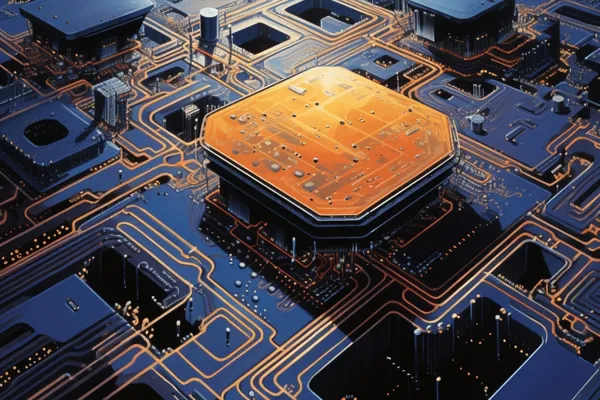
Although transistors soon replaced vacuum tubes as the main component of computers, the wiring of thousands of transistors remained intricate. It wasn't until 1958, when engineer Kilby built multiple "transistors" on the same silicon or germanium board to form an "integrated circuit" that its performance was greatly improved. And integrated circuits have another name - chips.
But soon, transistor miniaturization became an issue again.
In fact, as early as 1955, Bell Labs began to try to use photolithography technology to produce more sophisticated circuits on silicon wafers.
Bell Laboratories located in New Jersey, USA
At that time, the term "photolithography" did not exist, and this technology was called "photoengraving" or "etching". This is mainly because the principle of photolithography is similar to that of a camera. However, the photos taken by the camera are printed on the negative, while the photolithography technology "engravs" not photos, but circuit diagrams and other electronic components.
In 1958, American physicist Jay Lathrop and his assistant chemist James Nair were inspired by the microscope that they could make the image smaller by inverting the microscope, and used this principle to create tiny objects. Complex images are "printed" on the tabletop. As a result, "photolithography" technology began to be applied to semiconductor manufacturing.
For a period of time since then, the United States has been the leader in the lithography machine industry.
In the 1960s, the American GCA company manufactured the first contact lithography machine, which became a mainstream product at that time.
At this time, as the application range of semiconductors becomes increasingly wider, the market demand for lithography machines continues to rise. Japan's Nikon and Canon, which are the GCA supply chain, have also started the research and development of lithography machines.
Natlab, a small company owned by Philips in the Netherlands, also realized the opportunity and quickly launched a lithography machine manufacturing plan. It was the predecessor of the lithography giant ASML.
In 1967, Natlab developed a prototype lithography machine. Due to its advantages in precision technology and equipment, Natlab's lithography machine performs better than its peers in terms of accuracy, achieving a position movement of 10 centimeters with a displacement deviation of only 0.1 micron.
However, this technology did not receive widespread attention at the time. Instead, other endless technical problems made the mass production of photolithography machines difficult.
Until the early 1980s, the United States still maintained its advantage in the production of photolithography machines. In 1981, GCA's photolithography machine sales reached US$110 million, an increase of nearly 10 times in three years.
Japan's efforts were also fruitful. Nikon launched the first stepper lithography machine in 1980. This high-performance lithography machine was more stable and automated and quickly occupied the market.
At the same time, Natlab was almost sold because it couldn't make money.
At this time, ASML, a local chip equipment manufacturer in the Netherlands, stepped forward. In addition to photolithography machines, this company also produces all equipment related to chip manufacturing. Once the photolithography machines are integrated into the industrial chain, efficiency will be greatly improved. So in 1984, ASML was officially established.
After ASML's first CEO Jat took office, he solved the problem of mass production of photolithography machines by strictly controlling work processes and opening up the supply chain. At the same time, he also found that industrial upgrading has promoted the new generation of photolithography machines to improve the precision requirements for detail positioning, and ASML's technical advantages have finally begun to emerge.
After that, ASML's lithography machine sales gradually improved by relying on continuous investment in research and development funds, continuing to solve supply chain problems and opening up the market. In 1987, ASML benefited from its cooperation with TSMC. By 1989, its global market share reached 15%.
In 1991, ASML pioneered the use of modular design and parallel development, which not only greatly improved the production efficiency of photolithography machines, but also allowed customers to select various components at will, greatly improving production flexibility.
By the end of the 20th century, ASML’s only competitor was Nikon.
In the 1990s, in order to manufacture smaller transistors, the focus of competition among lithography machines became the wavelength of the light source.
At that time, Nikon and other companies advocated continuing the previous generation technology and taking a steady path, while TSMC's Lin Benjian came up with the "immersion lithography" solution that uses water to change the refractive index of light.
After Lin Benjian lobbied semiconductor giants in the United States, Japan and Germany to no avail, he hit it off with ASML. ASML quickly produced prototypes in one year and received a large number of orders. By 2004, the "immersion" lithography machine jointly developed by ASML and TSMC was born. This year, ASML began to counterattack.
However, the "immersion" lithography machine is still not enough to achieve the most refined processing on the chip. At this time, the lithography machine requires a light source with a smaller wavelength-extreme ultraviolet light. And ASML’s years of technological investment have just paid off.
As early as 1990, the United States gathered more than 50 units, including national laboratories, universities, and companies, to launch research and development of extreme ultraviolet light sources. However, due to the high technical difficulty and long R&D cycle, only ASML can continue to invest time and money.
Finally, in 2006, ASML produced more advanced EUV lithography equipment, further improving the performance of the chip. EUV lithography machines are tools used to produce key chips such as mobile phones, computers and various data processors.
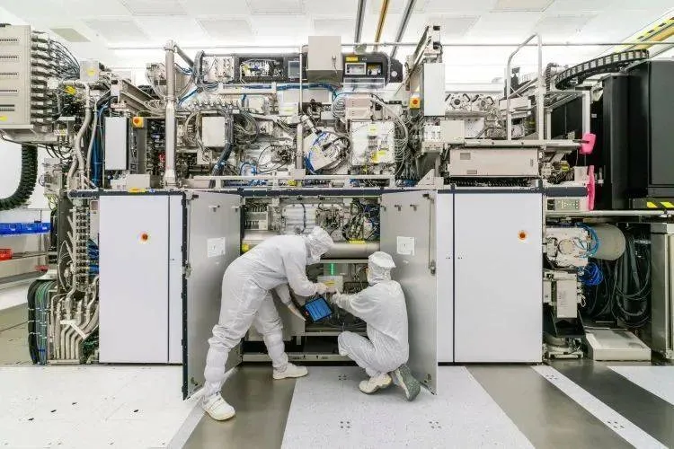
Engineers working in a clean room ASML official website
In fact, ASML was originally a small company. Its core competitiveness lies in integrating all aspects of invention, design and production to continuously iterate a very complex system.
To do this, the density of corporate knowledge needs to be large enough. Reggie Maker, director of the Netherlands High Technology Institute, believes that ASML is a knowledge-intensive enterprise. They are very good at system integration knowledge. The enterprise is also a laboratory that can absorb many new inventions.
The other is continued investment in all fields. Although ASML will still purchase key components from many suppliers, this does not prevent it from providing researchers with a large amount of research funds and time to study the corresponding components. This allows companies to obtain solutions as quickly as possible when facing industrial upgrading and technological challenges.